
Assembly Methods
Assembly methods for Powerelements on PCBs
The high current contact is the direct interface to the printed circuit board and an important component of power electronics. For each application, the high current contact, the PCB and the contacting method must be optimally matched.
Learn all about the assembly methods of our Powerelements here!
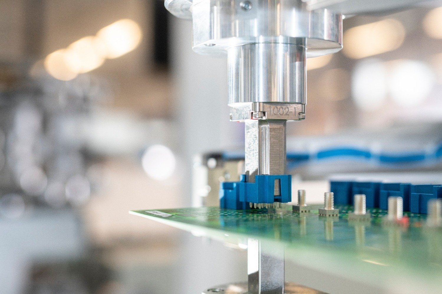
Assembly methods compared
| Assembly method | Massive Press-fit Technology (MPFT) | Flexible Press-fit Technology (FPFT) | Surface Mount Technology (SMT) | Through Hole Technology (THT) | Through Hole Reflow (THR) |
|---|---|---|---|---|---|
Product example |  |  |  |  |  |
Short description | Solid square pins are pressed into an electrically plated-through PCB hole. The PCB is deformed in the process and a gas-tight, cold-welded connection is formed along the length of the through-hole plating with a very high current carrying capacity. | Flexible pins are pressed into an electrically plated-through PCB hole. The pin deforms in the process. The gas-tight contact point is limited to the deformation zone of the pin. There is a wide range of design options for the shape of the pin. | The Powerelement is soldered to the surface of the PCB. The solder paste is applied to the PCB surface using a stencil. The solder pad is usually electrically connected to the different layers of the PCB using vias. | The solid pins are soldered into an electrically plated-through PCB hole. Either the circuit board is moved over the liquid tin (wave soldering) or the components are dipped into the liquid tin at specific points (selective soldering). The electrical connection is made through the solder. | The solid pins are inserted into the holes in the board filled with solder paste. As with SMT, the solder paste is applied to the PCB using a stencil. As the paste passes through the oven, it is melted and the pins are soldered into the hole. |
Assembly type * | Press-Fit | Press-Fit | Soldering | Soldering | Soldering |
Pins * | ✔ | ✔ | ✔ | ✔ | |
PCB-Tech IMS (Insulated Metal Substrate) * | ✔ | ||||
Surface ** | Tin (Silver) | Tin | Tin++ (Silver) | Tin+ | Tin++ |
Typical PCB surface *** | iSn, ENIG | iSn, ENIG | iSn, iAg, ENIG, OSP | iSn, iAg, ENIG, OSP | iSn, iAg, ENIG, OSP |
Typical packing **** | Bulk | Bulk | Bulk / Tray | Blister pack on reel | Blister pack on reel |
Product types |
* The overview shows a summary of the different methods of contacting the Powerelements in or on the PCB. Except SMT, all contact methods involve pins beeing pressed or soldered into the PCB. For PCBs with IMS (Insulated Metal Substrate) construction, only SMT contacting is suitable, as no holes can be drilled due to the metal core.
** Typical surface finishes for high current contacts are tin and silver. Surface coatings optimized for soldering technology are used for soldered parts and are designated Tin+ and Tin++. With Tin+ and Tin++ the soldered parts are again differentiated into the groups THT and SMT / THR.
*** The surface finish of printed circuit boards is often made in immersion tin or immersion nickel gold. Immersion tin is recommended for press-fit technology. Other finishes such as immersion silver or OSP (Organic Solderability Preservative) for soldering are also possible.
**** Press-fit components are normally supplied in bulk. Powerelements for the SMT / THT process are typically supplied in blister packs on reels due to processing on SMT lines. THT elements can be supplied in bulk, in trays or also in blister packs on reels.
Basics of assembly methods
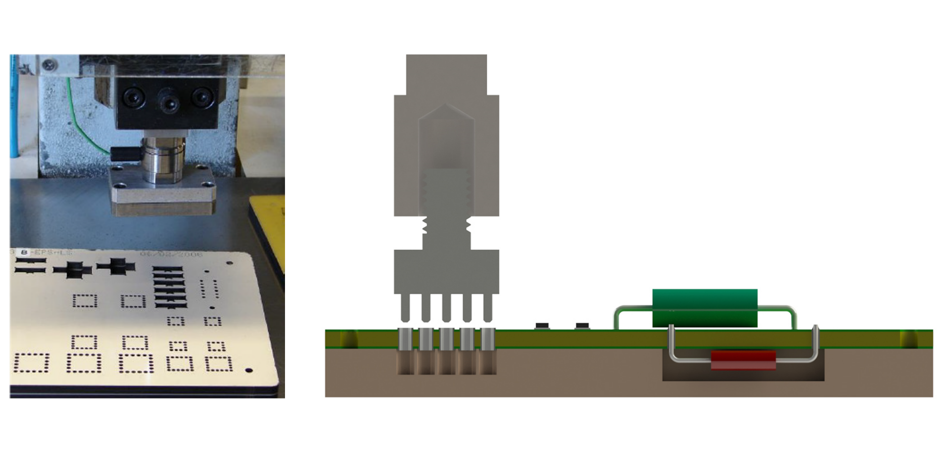
Basics of Massive Press-fit Technology (MPFT)
Massive Press-fit Technology, or MPFT, is the process of pressing rectangular or square solid pins into an electrically plated-through hole in a printed circuit board. During the process, the pin and mainly the PCB are deformed. Due to their excellent mechanical and electrical properties, press-fit Powerelements are particularly suitable for use under difficult conditions such as high temperature fluctuations or vibrations.
The quality of the press-fit connection is determined by the electrical contact resistance. The lower the resistance, the better the connection. Contact resistance generates a voltage drop and therefore heat, which is particularly problematic when carrying high currents. The press-fit process produces a high performance, gas-tight electrical connection with a contact resistance of a few μOhm.
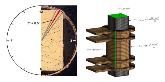
Micrograph and profile of a press-fit pin
To keep the contact resistance low, it is important to choose the right materials. The conductivity of copper (pin material CuZn39), which is many times higher than that of brass, means that with a PCB thickness of 2.4 mm, the connection angle of one corner of the contact pin to the copper sleeve of the PCB only needs to be at least 3°.
In order to achieve this contact angle, the component pin to be pressed must have a specially defined diagonal that is larger than the plated-through hole of the PCB.
Experience over the years has shown that the contact angle is significantly greater than the required 3°. It is clear that a massive press-fit zone provides an excellent electrical connection between a current feed element and a printed circuit board.
An example of the excellent values of press-fit technology
The massive press-fit technology of Würth Elektronik ICS is a very robust and reliable connection technology with one of the best FIT rates (FIT – Failure in Time).
Example:
- The contact resistance to the copper sleeve is 0.1 mΩ to 0.2 mΩ for a pin for the drill hole diameter 1.60 mm.
- The press-fit pin makes direct contact with the conductor track via the sleeve.
- A Powerelement with 36 press-fit pins therefore has 144 direct connections.
- If connections are made across several layers of the PCB, their number is multiplied.
This means that currents of several 100 amps can be fed in. The bottleneck is usually not in the connection to the PCB, but in the layout or connection area.
Features of the MPFT in conjunction with Powerelements
- Gas-tight welding of the contact points
- No thermal stress on the PCB due to the cold welding process
- Very high current carrying capacity due to low resistance contact points
- No risk of cold solder joints
- No flux residues
- High mechanical load capacity and vibration resistance
- Extreme long term stability against environmental influences
- Easy, cost-effective processing of very thick (high current) printed circuit boards with a high copper content
- Compact design of the assemblies possible due to double-sided assembly of the printed circuit board
Due to their excellent mechanical and electrical properties, press-fit assemblies are particularly suitable for use under difficult conditions, such as high temperature fluctuations or vibration.
General processing instructions MPFT in conjunction with Powerelements
- Press-in force: min. 60 N, max. 250 N per pin
- Holding force: 60 % to 80 % of the press-in force
- Press-in speed: 100–250 mm/min
- Temperature range: -40 °C to +150 °C
- No special press-in equipment is required for prototyping, a simple toggle press is sufficient.
- The PCB must be supported by a press-in pad during the press-fit process to avoid bending and / or damage to the PCB.
- The hole pattern in the press-fit pad must match the hole pattern in the product, with the holes being 0.3 mm larger. The drill holes must not be chamfered (More about drill hole specifications).
- The press force must be applied at a 90° angle to the PCB.
- A gap of 0.1 mm to 0.5 mm is recommended between the PCB and the socket.
- The pins should protrude from the PCB after pressing to fully contact the copper sleeve (> 0.2 mm).
- Through-hole plating of the PCB must be in accordance with our press-fit specifications.
- Components on the PCB should be approximately 4 mm from the Powerelement.
- The Powerelements and PCBs to be processed should be at room temperature.
- Use only suitable press-fit tools.
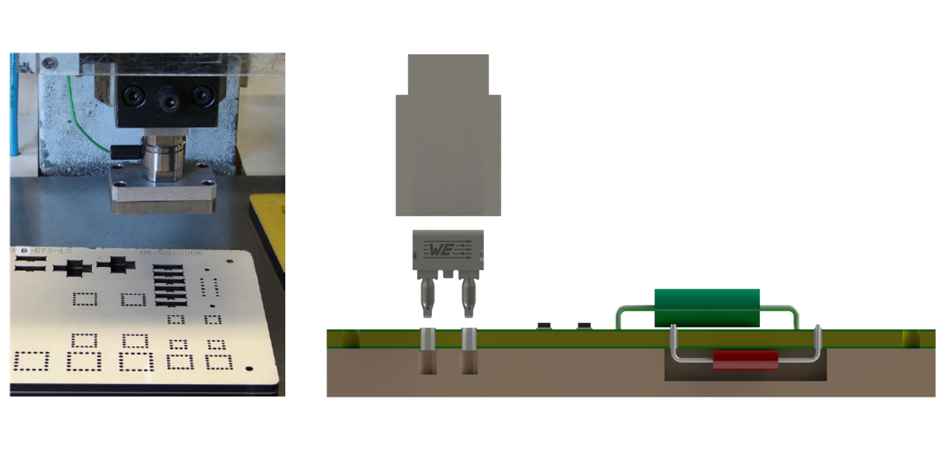
Basics of Flexible Press-fit Technology (FPFT)
Flexible Press-fit Technology(FPFT) involves pressing flexible pins into an electrically plated-through hole in the printed circuit board. This mainly deforms the pin. The gas-tight contact point is limited to the deformation zone of the pin and can limit the maximum current carrying capacity. There are a number of options for the shape of the pin, the most common beeing "needle eye".
Processing instructions FPFT in conjunction with Powerelements
- Press-in force: min. 60 N, max. 250 N per pin
- Holding force: 60 % to 80 % of the press-in force
- Press-in speed: 100–250 mm/min
- Temperature range: -40 °C to +150 °C
- No special press-in equipment is required for prototyping, a simple toggle press is sufficient.
- The PCB must be supported by a press-in pad during the press-fit process to avoid bending and / or damage to the PCB.
- The hole pattern in the press-fit pad must match the hole pattern in the product, with the holes being 0.3 mm larger. The drill holes must not be chamfered (More about drill hole specifications).
- The press-in force must be applied at a 90° angle to the PCB.
- A gap of 0.1 mm to 0.5 mm is recommended between the PCB and the socket.
- The pins should protrude from the PCB after pressing to fully contact the copper sleeve (> 0.2 mm).
- Through-hole plating of the PCB must be in accordance with our press-fit specifications.
- Components on the PCB should be approximately 4 mm from the Powerelement.
- The Powerelements and PCBs to be processed should be at room temperature.
- Use only suitable press-fit tools.
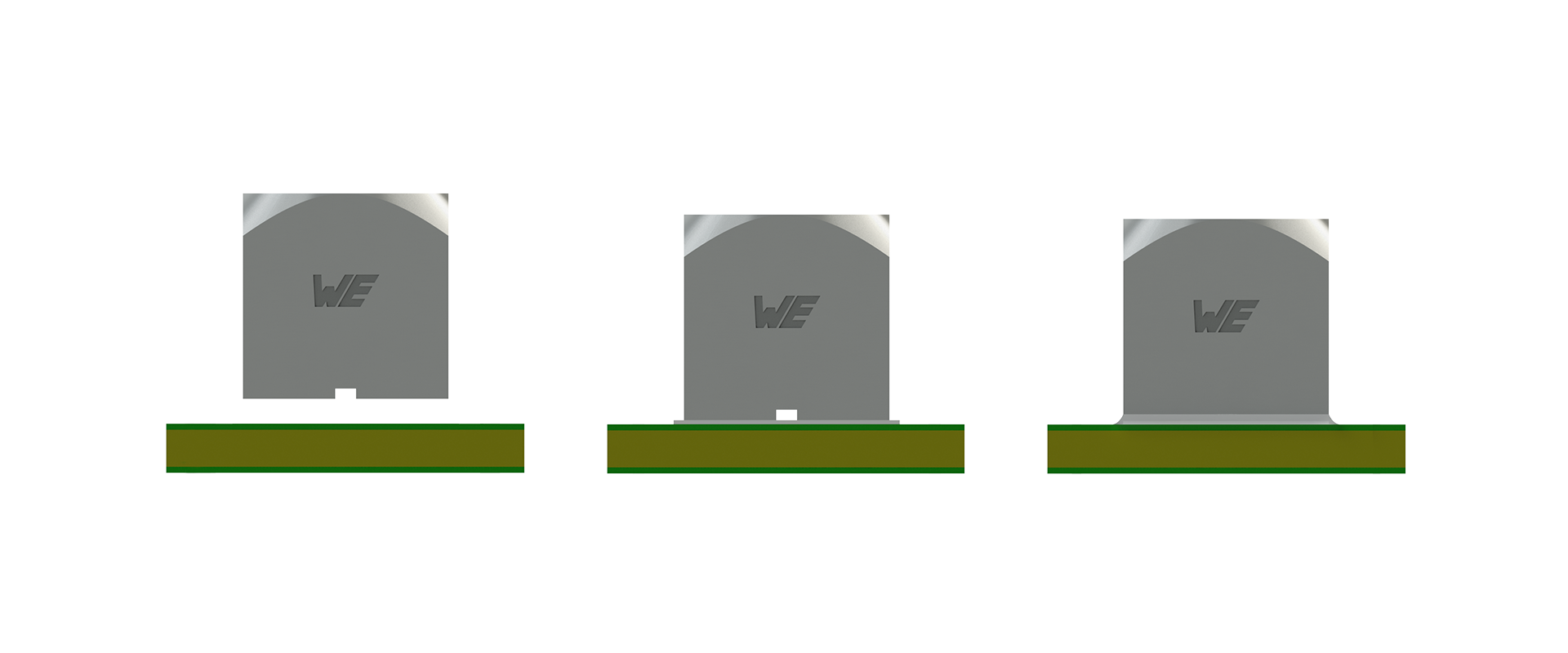
Basics of SMT process (Surface Mount Technology)
The SMT process involves soldering the component to the surface of the PCB. The solder paste is applied to the PCB surface using a stencil. Unlike the massive press-fit technology, the solder pad is usually electrically connected to the different layers of the PCB via vias.
Features of SMT in conjunction with Powerelements
- An SMT solder connection withstands the torques required for the screw connection.
- SMD components require a sufficient number of vias to distribute the current.
- Holes for the components are not provided (use IMS board).
Processing instructions for SMT in conjunction with Powerelements
- SMT / THR Powerelements can be processed in the typical SMT line and are soldered in the infrared oven or with the vapor phase system.
- Solder pad design according to product-specific specifications (min. 1 mm larger than footprint component).
- Through-hole plated or filled and sealed according to IPC 4761 Type 7
- Solder stencil design according to product specifications (approx. 0.2–0.3 mm smaller than solder pad).
- Solder paste thickness 150 μm.
- Soldering parameters according to the solder profile recommendation. Due to heat absorption by the mass of the components, own tests must be carried out to determine the parameters.
For more information on the soldering process, see: General notes on soldering technologies
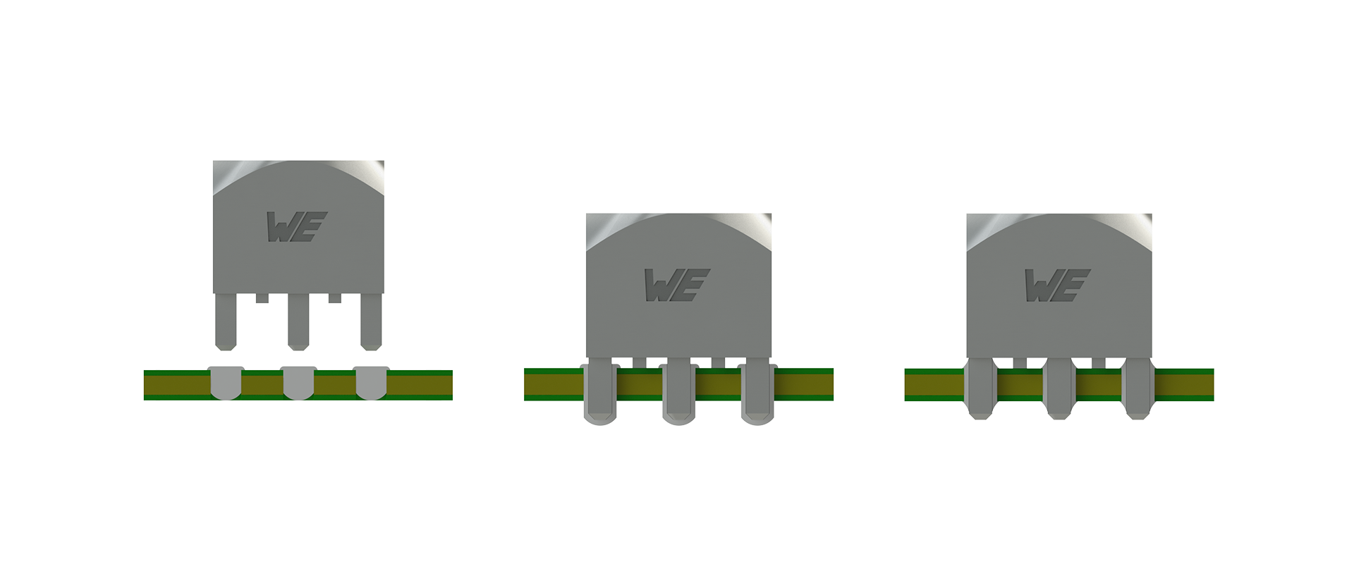
Basics of the THR process (Through Hole Reflow)
THR (Through Hole Reflow) technology is based on SMT technology. Here, the pins are placed in the plated-through holes of the PCB filled with solder paste. As with the SMT process, the solder paste is applied to the PCB using a stencil. As it passes through the oven, the paste is melted and the pins are soldered into the hole. The THR process is an alternative if no THT process is intended or selective THT is to be avoided.
Processing instructions for THR in conjunction with Powerelements
- SMT / THR Powerelements can be processed in the typical SMT line and are soldered in the infrared oven or with the vapor phase system.
- The vias on THR products must be filled with solder paste prior to reflow soldering. Wave soldering is not applicable.
- Solder parameters should be in accordance with the recommended solder profile. Due to heat absorption by the mass of the components, own tests must be carried out to determine the parameters.
- Final diameter of the through-hole plating according to the product specifications.
- Only the final diameter of the vias is relevant.
- The printed circuit boards should be designed according to IPC A 600, current edition
- Solder ring 500 μm around the through hole.
- Do not apply the solder pad over the entire surface (see general notes on soldering technologies)

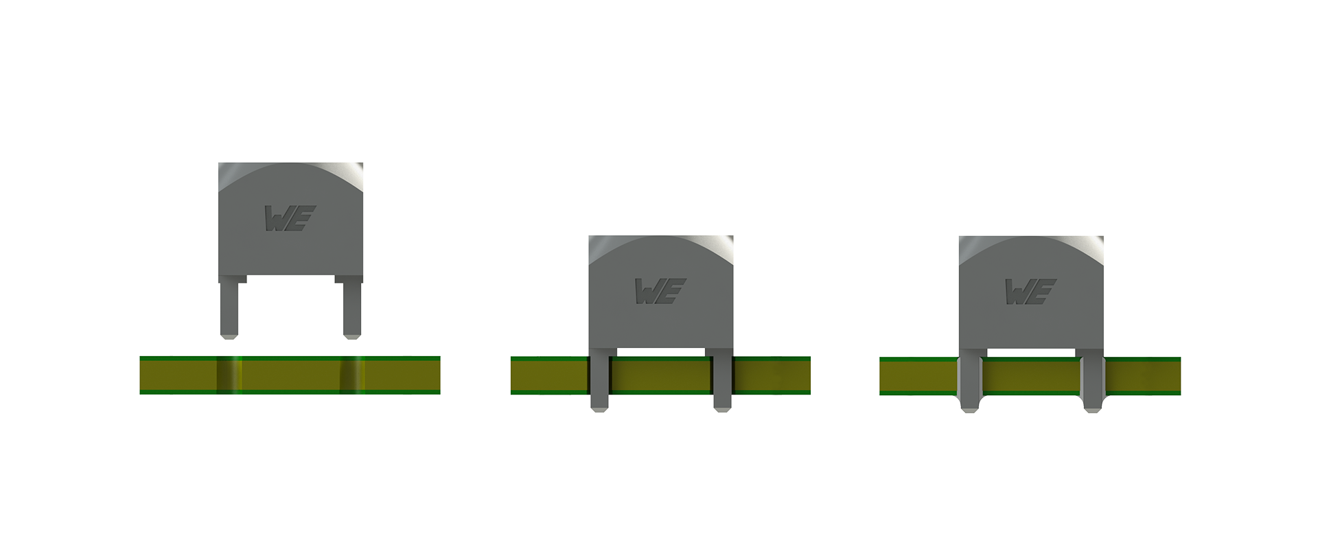
Basics of the THT process (Through Hole Technology)
The THT (Through Hole Technology) is the process of soldering solid pins into electrically plated-through holes in a printed circuit board. In wave soldering, the entire PCB is guided over a tin wave, while in selective soldering, the solder points are approached individually with a tin crucible. Compared to the massive press-fit technology, the solder joint has higher contact resistances, which can affect the current carrying capacity to be achieved. In addition, the solder joint has a poorer life test performance than massive press-fit technology.
Features of THT in conjunction with Powerelements
- THT high-current contacts can be loaded with the same torque as press-fit or SMT soldered Powerelements
Processing instructions for THT in conjunction with Powerelements
- THT products are manufactured for wave soldering. Soldering on SMT lines is not intended.
- Final diameter of the through-hole plating according to product specifications.
- Only the final diameter of the vias is relevant.
- The printed circuit boards should be designed according to IPC A 600, current edition
- Solder ring 500 μm around the through hole.
- Do not apply solder pad over the entire surface (see general notes on soldering technologies)

General notes on soldering technologies
| Priority | Value | Unit |
| Preheat temperature Ts min. | 150 | °C |
| Preheat temperature Ts max. | 200 | °C |
Preheat time ts from Ts min. to Ts max. | 75 | sec. |
| Ramp-up rate (TL to Tp) max. | 3 | °C/sec. |
| Liquidous temperature TL | 217–221 | °C |
| Time tL maintained above TL | 45–75 | sec. |
| Peak package body temperature Tp | 243 | °C |
| Time within 5 °C of actual peak temperature tp | 15 | sec. |
| Ramp-up rate (TL to Tp) max. | 6 | °C/sec. |
| Time from 25 °C to peak temperature max. | 300 | sec. |
Further information on soldering technologies is provided under solderability and storage of SMT / THT / THR Powerelements.
Connecting the component to the Powerelement
There are several ways to connect the Powerelement to the application side:
screwing, plugging and welding
| Connection options | Product example | Connection | Application |
|---|---|---|---|
Screwing |  | Bolt Bush |
|
Plugging |  | Bolt Bush |
|
Welding |  (The pictures shown are for reference only, the actual product may differ). | Plan (area) |
|
Connection options in detail
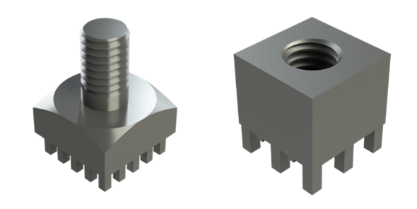
For screw connections, a threaded bolt or a threaded bushing is available for connecting a cable, a busbar or for fastening a component. Through-hole bushings allow the Powerelement to be screwed through, as it is common in IGBT connections. Through-hole threaded bushings allow for a lower overall height by reducing the overall height for a given thread length. In addition to the metric threads, Würth Elektronik ICS also offers Powerelements with UNC threads, fine threads and Helicoil® for the screw connection. Please take into account the note on the use of fastening materials.
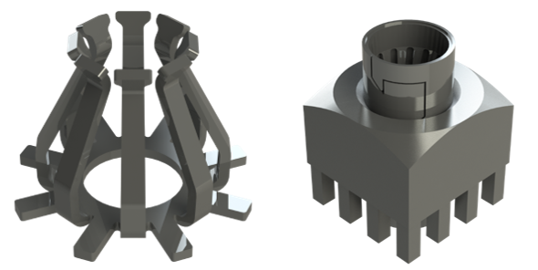
Pluggable solutions offer the advantage of quick assembly and easy disassembly. When using multiple connectors on a PCB, the required position tolerance must be considered. Some connector systems only allow a position tolerance of 0.1 mm, while connector systems such as the LF PowerBasket allow up to 0.6 mm.
When using mating connectors, attention must be paid to the optimum design of the contact tip, which affects the number of mating cycles that can be achieved. The LF PowerBasket family provides a cost-effective high current alternative to other pluggable high current solutions.
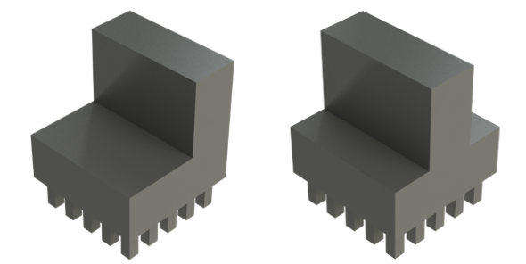
Welding components to high current contacts provides a robust connection that can withstand high currents. Welding firmly bonds the components to the contacts, ensuring a reliable electrical connection and minimizing potential problems such as corrosion.
For welded connections, material selection is important and should be project-specific. The zinc contained in standard brass interferes with the welding process and is not suitable for weldable Powerelements. The welding process used must also be considered.
(The pictures shown are for reference only, the actual product may vary).


